The Benefits that ESD Dust-free Wafer Mats Can Provide
Feb. 25, 2022
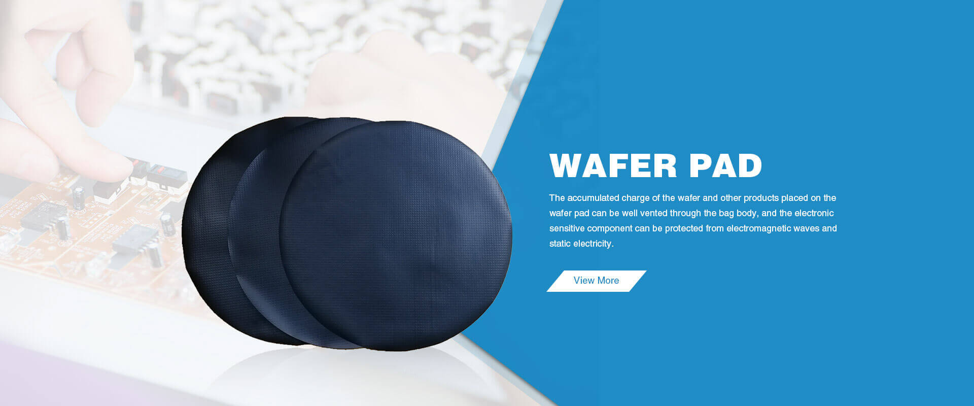
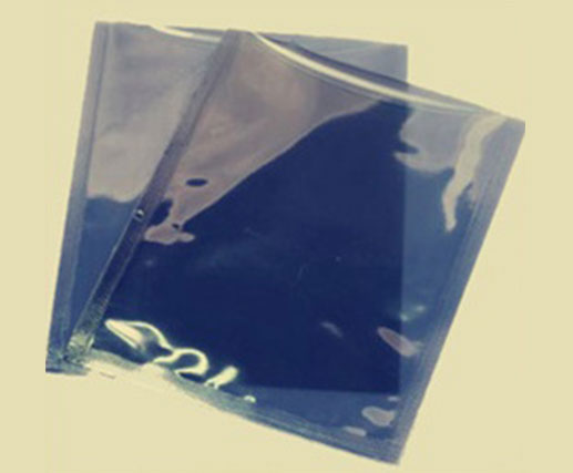
Wafer pad is also known as anti-static pad, anti-static sheet, conductive separator, black wafer separator, anti-static wafer separator, conductive wafer separator, wafer separator, black wafer pad, black wafer separator, round wafer pad, round wafer separator, wafer square, etc.
The accumulated charge of wafers and other products put on the wafer pad can be well discharged through the bag, which can protect the electronic sensitive components from the damage of electromagnetic waves and static electricity.
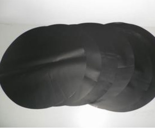
This product is made of permanent conductive or anti-static film after hot pressing into the pattern, die-cutting. The film surface can be made glossy, or various patterns can be made according to the requirements. The product can be made into any size and shape as required, and the finished product has excellent dimensional stability, neat appearance and no dusting. The raised patterned wafer pad can not only effectively prevent the product from damage by static electricity, but also play a certain buffering role.
●The surface resistivity can be adjusted between 3 times of 10 and 11 times of ohms as required.
●TONGXI can be made in any size and shape as required by customers
●Excellent dimensional stability, smooth surface, no powder and no dust.
●Good rigidity and toughness, good tensile strength and impact resistance.
●Adapted to a wide range of ambient temperatures as well.
●Static discharge time: <1.0 sec
These products are widely used in: clean room, clean room, photoelectric factory, LED factory, PCB factory, electronics factory, electrical factory, electronic instruments, wafers, LCD/LCM/LED, photoelectric optics, chip semiconductor, laser magnetic head, pharmaceutical chemicals, precision instruments, health care equipment, microelectronics industry, aerospace, military industry, electronic components (devices), photoelectric products, electronic devices, liquid crystal products, photoelectric integration products and other products aerospace manufacturing industry and other production areas that require ESD and purification level.
For semiconductor wafer foundry and TFT-LCD optoelectronics industry in the trend of large size of products and process microfabrication, due to the process of AMC (gas molecular pollutants) and VOC (volatile organic compounds) pollutants emitted, increasingly serious and more difficult to control. With the nanosize process of semiconductor components, these two sources of pollution have a great impact on the quality and yield of products.
Please contact us to get the quote.

