


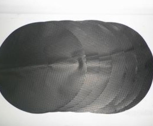
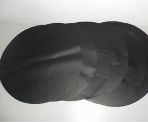
Wafer Pad
PRODUCT DESCRIPTION
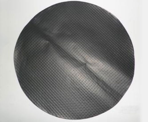
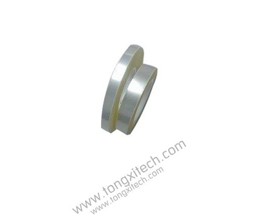
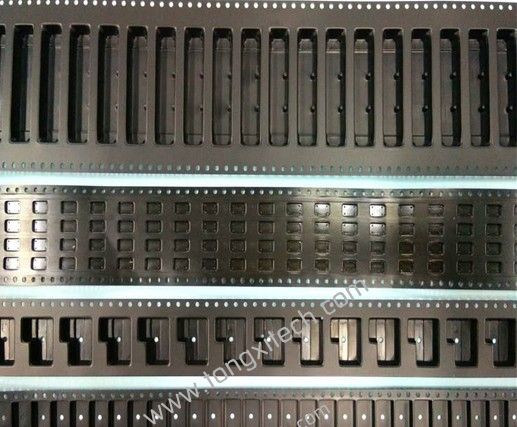
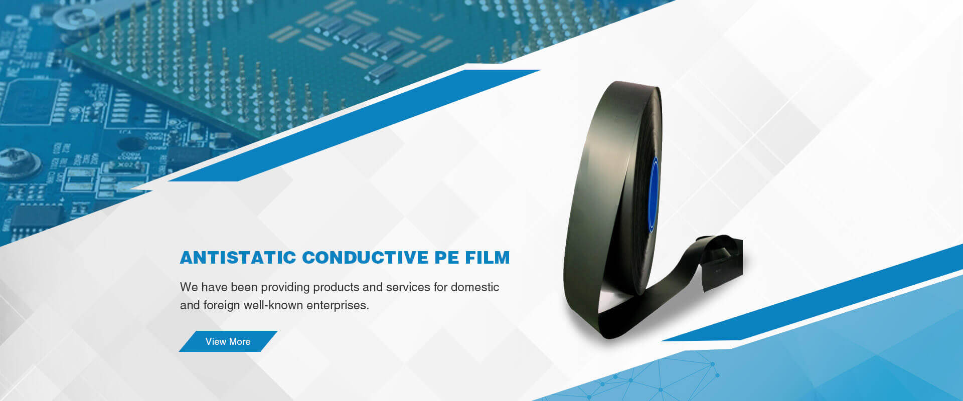
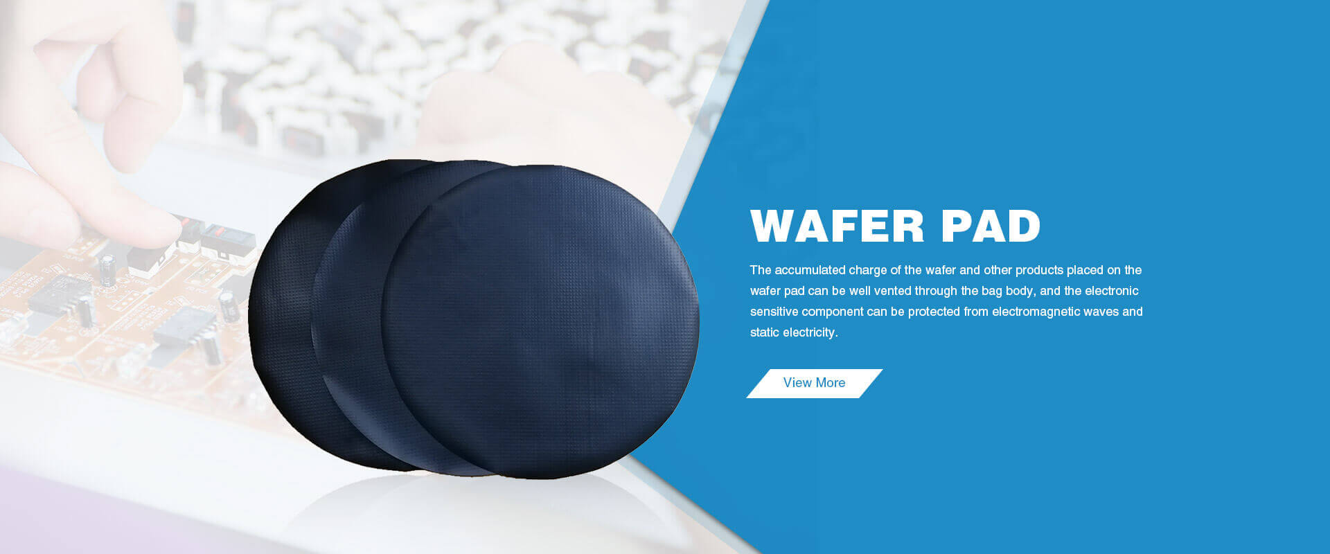
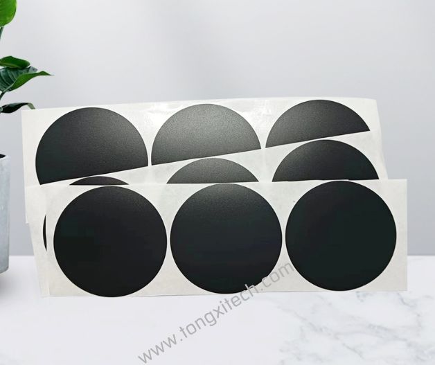
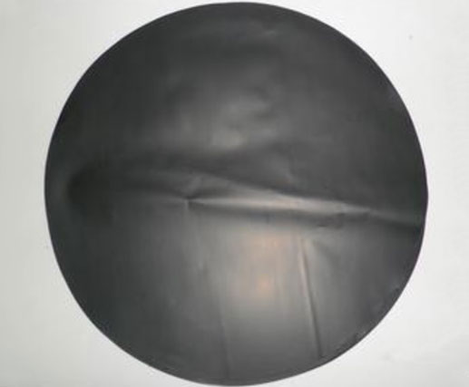
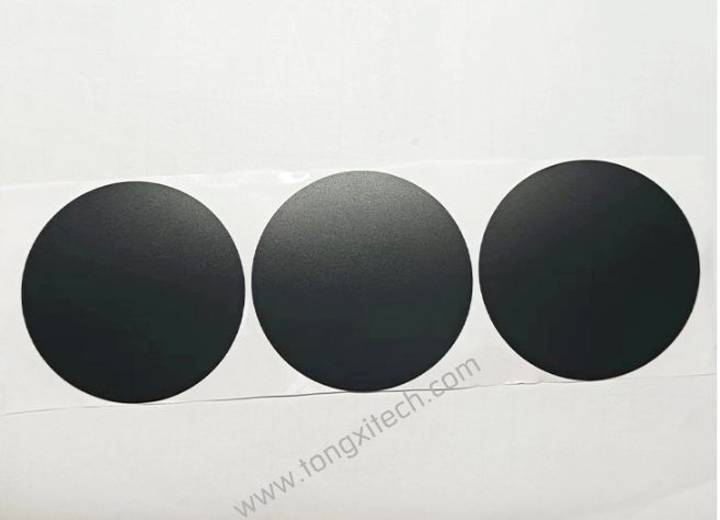
Tongxi manufactures ESD wafer pads and antistatic wafer separators for protecting sensitive wafers during handling, packaging, storage and transportation.
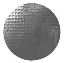
Available in conductive or static-dissipative PE and PS materials, our wafer pads help reduce static charge accumulation, prevent direct wafer-to-wafer contact and protect delicate surfaces from scratches, edge damage and contamination.
Custom sizes, thicknesses, shapes and embossed patterns are available for semiconductor wafers, solar wafers, glass substrates and other precision components.
Key Benefits
●The surface resistivity can be adjusted between 10^3-11Ω/Square as required;
●Can be made to any size and shape according to customer requirements;
●Excellent dimensional stability, smooth surface without dusting;
● has good rigidity and toughness and good tensile and impact resistance;
● The adapted ambient temperature range is also large;
●Static discharge time: <1.0sec
Available Materials
PE Wafer Pads
PE wafer pads are available for applications requiring flexible wafer separation, cushioning and custom die-cutting. Different conductive or antistatic formulations can be selected according to the required ESD performance.
PS Wafer Pads
PS wafer pads are suitable for applications requiring greater rigidity and dimensional stability. Thickness, diameter and surface embossing can be customized for different wafer containers and transportation systems.
The appropriate material should be selected according to wafer type, required rigidity, packaging structure, cleanliness requirements and ESD control plan.
Surface Options
Smooth Wafer Pads
Smooth pads provide a flat separation layer between wafers and are suitable for applications where a simple protective spacer is required.
Embossed Wafer Pads
Embossed surfaces reduce the contact area between the pad and wafer. They can help prevent sticking and improve separation during manual or automated loading and unloading.
Single-sided, double-sided, dot, grid and customized embossing patterns are available.
Applications
Tongxi wafer pads can be used for:
Semiconductor silicon wafer handling and packaging
Wafer storage boxes and shipping containers
IC wafer manufacturing and back-end processing
Solar wafer separation and transportation
LED, Mini-LED and Micro-LED substrate protection
TFT, LCD and precision glass substrate handling
PCB, ceramic substrate and precision component separation
Cleanroom storage and internal material transfer

Custom Wafer Pad Manufacturing
Provide the following information to receive an accurate recommendation and quotation:
Wafer or substrate material
Wafer diameter and thickness
Required pad diameter and shape
Required pad thickness
PE or PS material preference
Target surface resistance
Smooth or embossed surface
Cleanliness or particle requirements
Operating temperature
Required quantity and packaging method
Our team can produce samples for dimensional, handling and packaging evaluation before mass production.
Why Choose Tongxi?
Experience supplying materials for semiconductor and electronic packaging
PE and PS wafer pad manufacturing options
Custom resistance, thickness, diameter and embossing
Sample and small-batch evaluation support
Stable production and lot inspection
Export packaging and international delivery support
Responsive technical and quotation service
Frequently Asked Questions
What is the difference between a wafer pad and a wafer separator?
The terms are commonly used for the same type of product. Other names include wafer spacer, antistatic wafer separator, conductive wafer pad and wafer interleaf.
Can you manufacture pads for different wafer sizes?
Yes. Diameter, shape, thickness and center-hole design can be customized according to the wafer, carrier or shipping container.
Are smooth and embossed surfaces available?
Yes. Smooth, single-sided embossed and double-sided embossed pads are available. The embossing pattern can also be customized.
How should I select the surface resistance?
The target resistance depends on the ESD control plan, wafer sensitivity, handling environment and packaging system. Please provide your required resistance range or application details for material selection.
Request a Custom Wafer Pad Quote
Send us your drawing, wafer diameter, pad thickness, material preference, resistance requirement and estimated quantity.
Tongxi will recommend a suitable ESD wafer pad specification and provide a quotation for sample or mass production.