



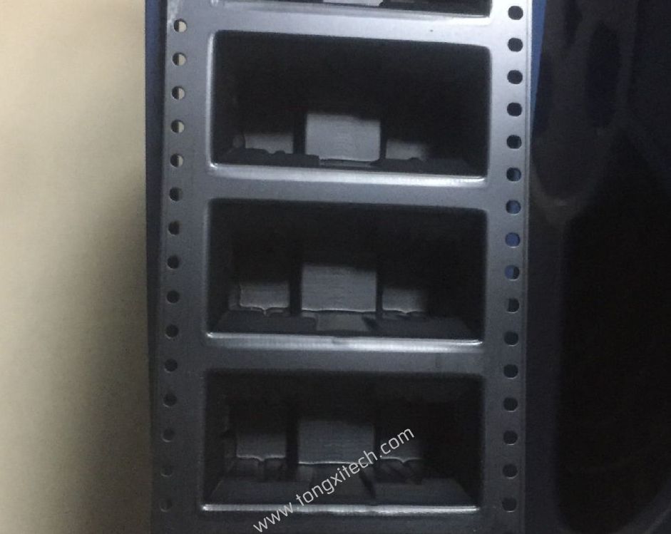
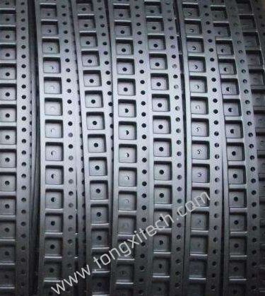
Carrier Tape
PRODUCT DESCRIPTION
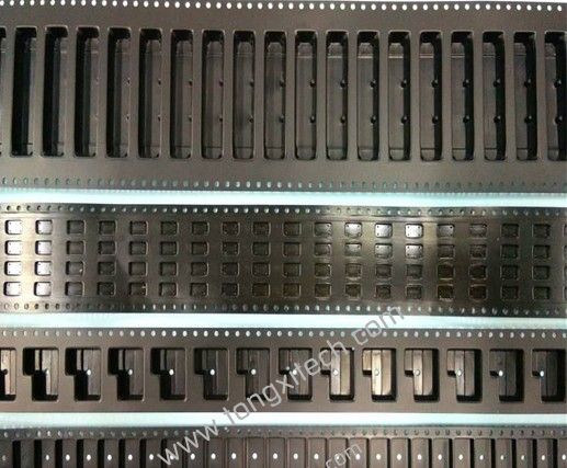
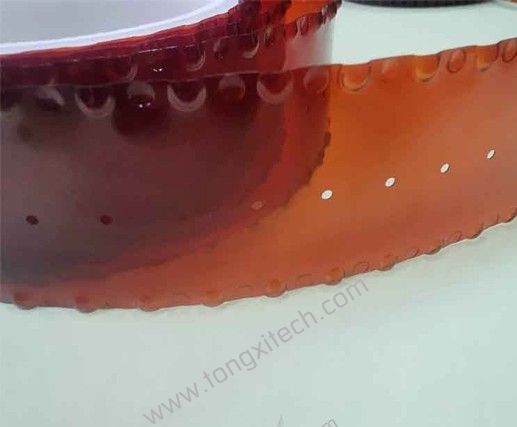
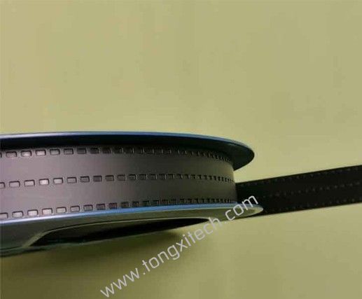
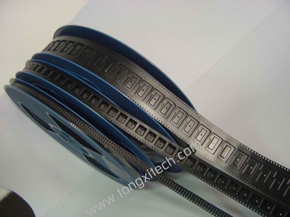
The Embossed carrier tape is an essential packaging material designed for high-speed automated taping systems and surface-mount technology (SMT) equipment. Manufactured using high-quality PS and PC materials, Tongxi Carrier Tapes offer excellent dimensional accuracy, stability, and durability. With a range of standard sizes available, they are ideal for protecting electronic components during transportation, automated assembly, and storage.
Tongxi Electronics manufactures embossed carrier tape from PC (polycarbonate), PS (polystyrene), and PET (polyester) base materials. All tape dimensions conform to EIA-481 sprocket hole and pocket geometry standards, ensuring direct compatibility with Yamaha, Fuji, Juki, Panasonic, and all other major SMT feeders. Custom cavity designs are supported with tooling lead times of 10–15 business days.
Technical Parameters
| Parameter | Specification |
|---|---|
| Material | PS, PC,PET |
| Standard Widths | 12 / 16 / 24 / 32 / 44 mm |
| Pocket Accuracy | High-precision forming, customizable |
| Surface Options | Anti-static / Conductive / Standard |
| Compatibility | SMT pick-and-place & automated taping machines |
Product Features
High-Quality Materials (PS & PC):Made from durable and stable Polystyrene (PS) and Polycarbonate (PC), the carrier tapes ensure strong protection and consistent performance.
Precision-Formed Pockets:Each pocket is formed with high dimensional accuracy, preventing component movement and ensuring compatibility with high-speed automated taping equipment.
Stable & Reliable Performance:Designed for SMT applications, Tongxi carrier tapes maintain their shape, resist deformation, and provide excellent component retention.
Wide Size Compatibility:Available in multiple standard widths to support various component sizes, offering versatility across multiple industries.
Optimized for Automation:Perfectly matched for high-speed pick-and-place machines and automated packaging systems, guaranteeing smooth feeding and consistent operation.
Product Specifications
Material Options:
Choosing the right base material for embossed carrier tape determines pocket dimensional stability, ESD performance, and process compatibility. The three materials we offer address different production requirements:
| Material | Key Properties | Best For |
|---|---|---|
| PC (Polycarbonate) | Heat deflection ≥85°C (0.45MPa); high rigidity; lower post-form shrinkage; excellent impact resistance | IR reflow soldering processes; ICs and precision die where pocket stability is critical; ESD-sensitive CMOS components |
| PS (Polystyrene) | Cost-efficient; good transparency for visual inspection; easy to form | Standard SMT passives (resistors, capacitors, LEDs); ambient-temperature transport; high-volume cost-sensitive applications |
| PET (Polyester) | Superior moisture and chemical resistance; stable dimensions across humidity ranges | Long-term storage; harsh logistics environments; components sensitive to moisture ingress |
All three materials are available in anti-static grades (surface resistivity <1×10¹¹ Ω, ANSI/ESD STM11.11) for ESD-sensitive devices.
Standard Widths:
12mm
16mm
24mm
32mm
44mm
Surface Features: Anti-static or conductive options available upon request
Pocket Design: Precision pocket dimensions, customizable for specific components
Applications:
SMT component packaging
Automated pick-and-place
Electronics transportation & storage
Semiconductor component protection
Applications
Tongxi Carrier Tape is widely used across the electronics and semiconductor industries, including:
Surface-Mount Technology (SMT):Ensuring stable placement and delivery of components for automated assembly lines.
Semiconductor Packaging:Protecting ICs, chips, LEDs, and micro-components during logistics and production.
Consumer Electronics:Ideal for resistors, capacitors, transistors, sensors, LEDs, and other small devices.
Automotive Electronics:Ensuring stable packaging for critical high-reliability components.
Communication Equipment Manufacturing:Supporting the high-speed assembly of RF modules, network chips, and micro-circuits.
Custom Embossed Carrier Tape — Design to Delivery
Tongxi supports both standard and non-standard embossed carrier tape designs. The custom development process:
Step 1 — Submit Component Drawing or Sample
Send us your component drawing (2D/3D) or a physical sample. Key dimensions we require: length × width × height of the component, lead/bump clearance if applicable, and orientation requirements.
Step 2 — Cavity Design & Engineering Review
Our team designs the pocket geometry — including cavity dimensions, draft angle, wall thickness, and sprocket hole layout — ensuring correct component fit, orientation lock, and cover tape sealing compatibility.
Step 3 — Tooling Fabrication
Forming tool is manufactured in-house. Standard tooling lead time: 10–15 business days.
Step 4 — Sampling & Validation
We produce a sample run (≤5 meters) and ship for your fit-and-function test. Dimensional report and surface resistivity test data included.
Step 5 — Mass Production
Upon sample approval, we proceed to production. Batch CoC and test report issued with every shipment.
Customizable parameters: cavity shape and depth, tape width, material and color, anti-static level (standard / dissipative / conductive), pocket pitch, reel length, and printed marking.
How Embossed Carrier Tape Works in SMT Production
Understanding how embossed carrier tape integrates into an automated line helps purchasing teams and process engineers specify the correct configuration:
1. Component Loading — Components are loaded into individual pockets of the embossed carrier tape by tape-and-reel packaging equipment. Each pocket holds exactly one component in a defined orientation.
2. Cover Tape Sealing — A heat-seal cover tape is applied over the loaded carrier tape at 130°C–170°C, creating a closed, protected package. Tongxi supplies pre-validated matched carrier tape + cover tape sets to eliminate seal compatibility issues.
3. Reel Winding — The sealed tape is wound onto a plastic reel (7-inch or 13-inch), forming the finished tape-and-reel component package for shipment.
4. SMT Feeder Loading — The reel is loaded into an SMT feeder. The feeder's sprocket engages the tape's index holes (EIA-481 4mm pitch) to advance the tape by one pocket per cycle with ±0.1mm positional accuracy.
5. Cover Tape Peeling & Pick — The feeder peels the cover tape back, exposing each component pocket at the pick point. The pick-and-place head lifts the component and places it on the PCB. Consistent pocket geometry is critical here — pocket wall deviation directly causes mis-pick events.
6. Trailer Exit — After all components are consumed, the trailing empty section (leader tape, min. 200mm per EIA-481) allows the feeder to complete the last pick cycle cleanly without jamming.
Frequently Asked Questions
Q1: What is the difference between embossed carrier tape and paper carrier tape?
Embossed carrier tape uses thermoformed plastic pockets that hold the component on all sides — top, bottom, and walls — preventing tilt, flip, and migration. Paper carrier tape uses punched flat holes and relies on the cover tape to retain the component from above only. Embossed tape is required for tall, heavy, or irregularly shaped components, for any reflow-compatible application, and wherever ESD protection is needed. Paper tape is appropriate only for very small, flat passives (e.g., 0201/0402 chip components) where cost is the primary driver.
Q2: How do I specify the correct pocket depth for my component?
The pocket depth should be the component height plus a clearance of 0.1mm–0.3mm to prevent jamming, but not so deep that the component can tilt freely. As a rule: pocket depth = component max height + 0.15mm (typical). For components with leads or bumps, measure the full seated height. Send us your component drawing and we will recommend the correct depth with a sample for validation.
Q3: Which material should I choose for components that go through IR reflow soldering?
Specify PC (polycarbonate) embossed carrier tape. PC has a heat deflection temperature ≥85°C under load, meaning the pocket geometry remains stable during reflow oven pre-heat stages. PS softens at lower temperatures and is not suitable for on-reel reflow processes. PET is reflow-compatible in some formulations but PC remains the industry default for this application.
Q4: Can I use anti-static embossed carrier tape for all ICs, or only specific device types?
Anti-static (dissipative) carrier tape with surface resistivity in the 10⁶–10⁹ Ω range is suitable for most standard ICs and passives. For highly sensitive devices — CMOS logic, RF ICs, power MOSFETs, and bare die — specify our conductive grade (10³–10⁵ Ω), which provides a faster static decay path. If in doubt, we recommend the conductive grade as it provides stronger protection without any feeding performance penalty.
Q5: Is your embossed carrier tape compatible with all SMT feeders?
Yes. All Tongxi carrier tape dimensions conform to EIA-481-D, the universal dimensional standard for tape-and-reel SMT packaging. Sprocket hole diameter (1.5mm +0.1/–0mm), hole pitch (4mm), and edge clearances are held to standard tolerances, ensuring direct compatibility with Yamaha, Fuji, Juki, Panasonic, Samsung, and other major feeder systems.
Q6: Do you provide samples before a production order?
Yes. Free samples of up to 5 meters are available for standard sizes. For custom cavity designs, samples are produced after tooling fabrication (10–15 business days from drawing submission) and shipped with a dimensional inspection report and surface resistivity data. No production order is required to receive samples.
At Tongxi, we are committed to providing high-precision carrier tapes that optimize your automated packaging performance.
For orders, technical support, or customized solutions, please contact us today – our team is ready to assist you!