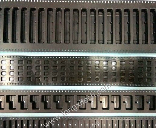
Wafer Pad PS
PRODUCT DESCRIPTION
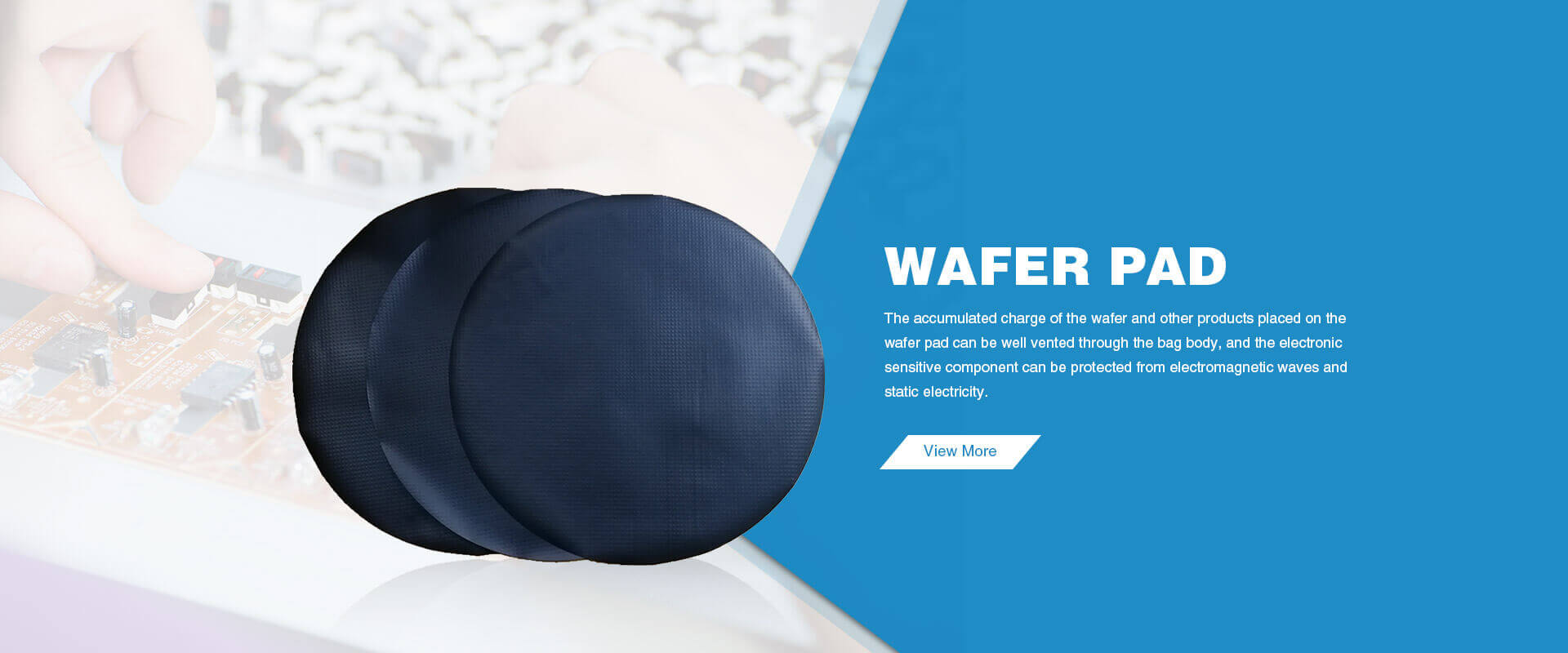
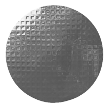
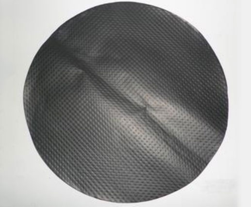
Anti-Static Wafer Pad PS is an anti-static packaging material specially designed for semiconductor wafers, which is mainly used to prevent damage to wafers caused by static electricity accumulation and discharge during storage, transportation and processing.
Material and Properties:
Anti-Static Wafer Pad PS is mainly composed of anti-static polystyrene (PS) material, which undergoes special processing to enhance its electrostatic dissipation properties. Its surface resistivity is typically maintained between 10^5 and 10^9 ohms/square to effectively prevent the buildup of static electricity.
The PS material itself exhibits strong mechanical characteristics such as moderate hardness, impact resistance, light weight, and ease of molding and processing, making it well-suited for the precise packaging needs of semiconductor wafers.
Product Details
| Specification | Description |
|---|---|
| Model | Anti-Static Wafer Pad PS |
| Material | High-quality Polystyrene (PS) |
| Color | Black |
| Size | Customizable: Can be made according to customer needs |
| Thickness | 160±16μm |
| Anti-Static Effect | High anti-static capability, meeting IPC-610 standards |
| Load Capacity | Capable of bearing heavy wafers, ensuring no damage |
| Applicable Industries | Semiconductor, IC, Smart Cards, Chip Manufacturers, Optoelectronics, etc. |
| Certification | ISO 9001 Certified |
| Product Features | High quality, stable performance, strong abrasion resistance, strong anti-static capability |
| Applicable Equipment | For the manufacturing and transportation of wafers, chips, ICs, smart cards, etc. |
| Production Process | Automated production with strict quality control and carefully selected raw materials |
Advantages of Anti-Static Wafer Pad PS
Static Electricity Issue: Effectively prevents static build-up, ensuring products are not affected by static during production and transportation.
Load Capacity and Safety: Strong load-bearing capacity, ensuring safety during transportation of wafers and ICs.
Material and Customization Needs: Offers multiple thicknesses and sizes to meet different customer needs.
Quality Assurance and Stability: ISO 9001 certification ensures stable and reliable product quality.
Why Choose Tongxi Anti-Static Wafer Pads?
Tongxi Electronics Technology Co., Ltd. was founded in 2010, and has been a professional processing and export enterprise specializing in supporting production materials for IC, smart card, chip, and semiconductor manufacturers. Our company is committed to providing high-quality products and services with an integrated quality control system. We are ISO 9001 certified, ensuring the highest standards in every product we deliver.
Competitive Price & High-Quality Products: Cost-effective pricing with top-tier quality.
Global Recognition: Trusted by industry leaders like STMicroelectronics, Eastcompeace, Apollo, Smartflex.
Automated Production & Quality Control: 5000 sqm factory with automated production lines and state-of-the-art testing equipment.
Reliable Service: Comprehensive post-sale support and a focus on customer satisfaction.
Proven Expertise: Over a decade of industry experience in semiconductor and electronics manufacturing.
We welcome the opportunity to cooperate with you. Contact us today!
Tags: Cover Tape, Carrier Tape, Spacer Tape, Leader Tape, Black Conductive PE film, Electronic Plastic Reel, Wire Bond Tools.

