



What Are Wafer Pads Used For in Semiconductor Packaging?
Sep. 18, 2026
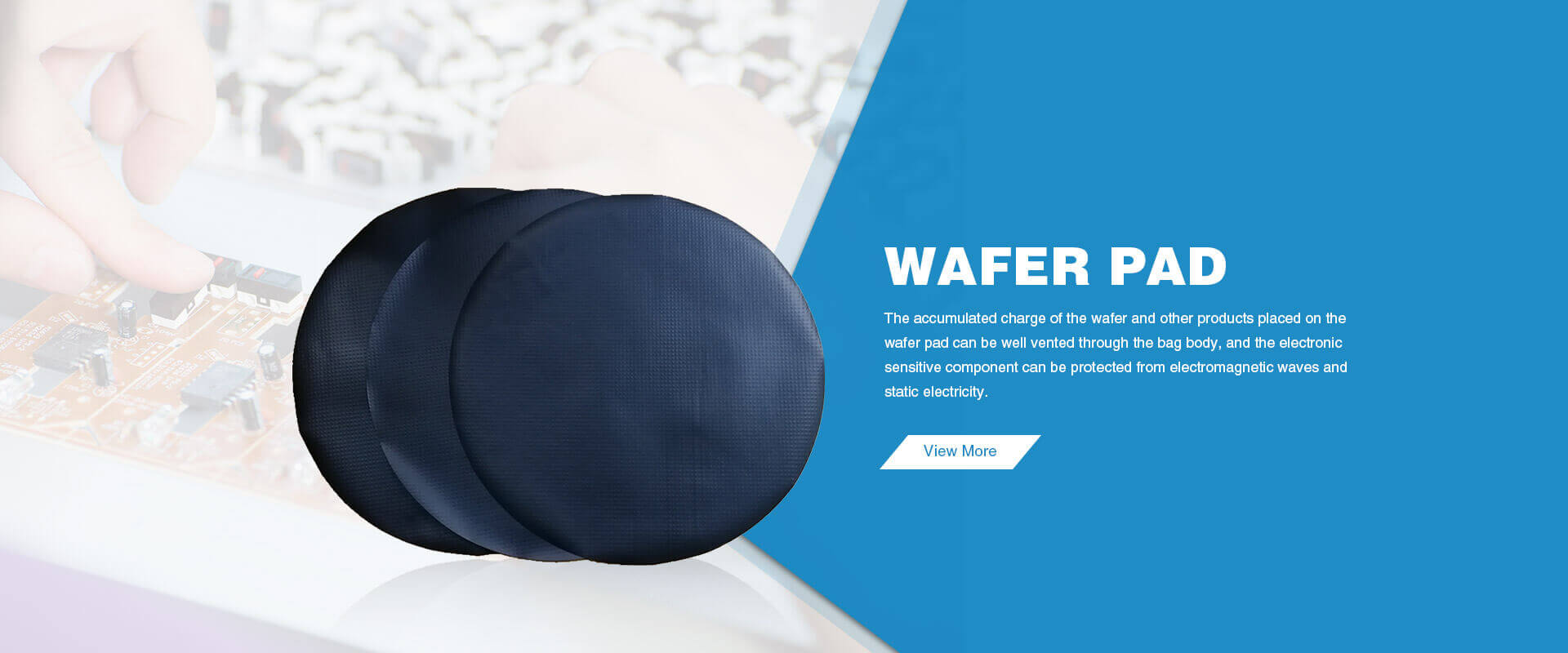
In the fast-evolving semiconductor industry, Wafer pads serve a crucial role in enhancing production efficiency and protecting delicate silicon wafers during processing. As the demand for miniaturization and increased performance escalates, advanced materials like wafer pads have emerged to address significant pain points. Specifically, manufacturers are experiencing challenges with wafer fragility, contamination risks, and the need for efficient handling processes. Wafer pads provide solutions that not only safeguard wafers but also improve yield rates in semiconductor packaging, making them essential tools in the industry.
Definition
Wafer pads, often referred to as carrier pads or process pads, are specialized soft materials used in the semiconductor manufacturing process. These pads serve to cushion and support silicon wafers during various stages, including cutting, grinding, and packaging. The industry terms associated with wafer pads include “wafer handling,” “dicing,” and “adhesion.” They are crafted from materials such as polyurethane, silicone, and other polymers that provide both cushioning and non-slip properties.
Application Scenario
Wafer pads find applications across various fields within semiconductor packaging, including:
- Dicing and Cutting: In the initial stages of semiconductor manufacturing, wafer pads support wafers during dicing processes, minimizing breakage risks.
- Grinding: During the grinding phase, wafer pads hold wafers securely while allowing for precise adjustments, which can increase manufacturing accuracy up to 45%.
- Transport and Storage: Wafer pads are vital during the transport of wafers in cleanroom environments, where contamination can exceed acceptable levels, typically measured around 1 defect per 1,000 wafers in controlled environments.
These applications underline the importance of using high-quality wafer pads that can adapt to the specifics of different processes while ensuring wafer integrity.
Brief Description of Advantages
The importance of wafer pads cannot be overstated in the semiconductor industry. Among their numerous advantages, consider the following:
-
Reduction in Defects: Utilizing wafer pads during processing has been shown to improve yield rates by 20% by minimizing breakage and defects that could occur through handling and processing.
-
Enhanced Cleanliness: Wafer pads create a barrier against contaminants, significantly decreasing contamination levels. This is critical, as semiconductor defects stemming from particles can lead to costly issues, often measured in thousands of dollars per defective unit.
-
Efficiency Gains: The implementation of wafer pads can lead to an increase in operational speed by reducing the time required for handling and processing, such as moving wafers through grinding—measured at a 30% efficiency improvement.
-
Versatility: Wafer pads are applicable across various semiconductor processes, making them a cost-effective choice amid increasing production demands.
Next Step Guidance
To fully utilize wafer pads in your production line, review the user guide provided by manufacturers like Tongxi, which outlines proper installation and maintenance practices. Understanding the specific properties of different pads will enhance manufacturing processes and ensure maximum efficiency and protection for your wafers.
FAQ
What is the lifespan of wafer pads? Wafer pads typically have a lifespan of more than 500 cycles depending on the workload and handling conditions. Regular inspection is necessary to maintain optimal performance.
How do I choose the right wafer pad for my process? Selecting the right pad involves evaluating the specific type of processing, the size of the wafers, and the required cushion properties. Consult with suppliers for detailed specifications.
Can wafer pads affect production speed? Yes, wafer pads can enhance production speed by streamlining processes and reducing handling time. Studies have measured speed improvements by up to 30%.
Where can I try high-quality wafer pads? Consider exploring products from established brands like Tongxi, known for their innovative solutions in semiconductor manufacturing.
By understanding and integrating wafer pads into semiconductor packaging, manufacturers can significantly advance their production capabilities while mitigating the risks associated with wafer handling.